
5.1 Sub-Panel/Production Formats
Sub-Panel Design
Sub-Panels
Production Formats
Single Sub-Panel
Sub-Panel Within Production Format
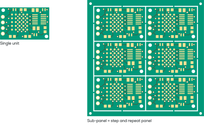
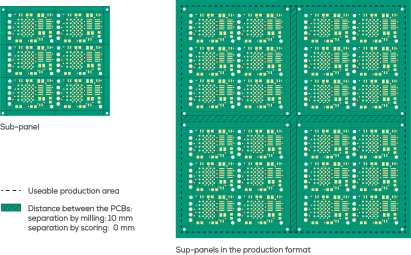
| Sub-panel types | Learn more under |
|---|---|
| Milled sub-panel | 5.2 Sub-Panel Design| Milled Sub-Panel |
| Scored sub-panel | 5.3 Sub-Panel Design | Scored Sub-Panel |
| Panel Combination scored-milled sub-panel | 5.4 Sub-Panel Design | Scored and Milled Sub-Panel |
| Example of sub-panel and material utilization | 5.5 Sub-Panel Design | Example of Material Utilization |
| PCB Technology | Usable Production Area / Formats |
|---|---|
| Double-sided PCBs | 578 × 498 mm; 573 × 500 mm; 578 × 428 mm; 573 × 426 mm |
| Multilayer PCBs | 578 × 498 mm; 573 × 500 mm; 578 × 428 mm; 573 × 426 mm |
| HDI/SBU PCBs | 578 × 498 mm; 573 × 500 mm; 578 × 428 mm; 573 × 426 mm |
| High-frequency PCBs | 578 × 498 mm; 578 × 428 mm; 573 × 426 mm |
| Semi-flex PCBs Rigid-flex PCBs |
578 × 428 mm; 573 × 426 mm |
| Rigid-flex PCBs Four Flex Layers |
573 × 426 mm |
| Heavy Copper PCBs Iceberg PCBs Copper IMS PCBs |
573 × 426 mm |
| HSMtec© PCBs | 578 × 498 mm; 578 × 428 mm |
| Embedded Technology | 573 × 426 mm |
Note for practical impedance control learn more: Observe maximum space loss of 200 × 23 mm per measurement coupon.
Minimum/maximum PCB size
The minimum PCB size can be a few millimeters, square or round, but is then packaged as so-called bulk goods. To enable normal packaging variants learn more about packaging variants and also automated final cleaning/rinsing, a minimum PCB size of ideally 50 × 50 mm, advanced 50 × 30 mm, is required.
The maximum PCB size is usually the usable area (net-area) according to the production format table, depending on the PCB technology. Due to the width of the shrink wrap for the standard packaging variant, the maximum width is limited to 450 mm. PCBs with greater widths up to the maximum width according to the table of production formats are given special packaging.
Keywords
- Sub-panel
- Production panel formats
- X-outs
- Panel border
- Breakaway tabs
- PCB size
- Depaneling
- Panelization