10.5 HAL (Lead-Free/Leaded)
| Feature | Description / Value |
|---|---|
| Application |
|
| Properties |
|
| Properties of lead-free HAL |
|
| Properties of leaded HAL |
|
| Plating thickness [µm] | Surface: 1 - 30 Hole < 3.0 mm: 1 - 50 Hole ≥ 3.0 mm: 1 - 70 |
| Processing warranty in months (at a max. storage temperature of 30°C and max. relative humidity of 70%) | 12 |
| Not to be used on |
|
| Not recommended for |
|
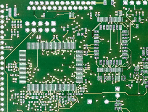
Wetting problems with insufficient Font-weight in Copper areas
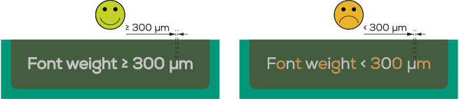
Perfect tin wetting of lettering on copper areas can only be guaranteed with a font-weight of at least 300 µm!
Wetting problems of SMD pads in copper surfaces


Perfect tin wetting of such SMD pads fully connected in larger copper surfaces with the HAL (Hot Air Leveling) surface is not always guaranteed! The reason lies in the thermal behaviour of such SMD pads, as the heat introduced by the HAL (Hot Air Leveling) process is quickly conducted (spread) into the copper area, making it difficult for these SMD pads to reach temperature!
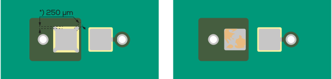
*) Design proposal for Thermal pads, if there are no other special requirements.
The four connections should be rotated by 45°.
The four connections should be rotated by 45°.
Frequently asked questions
Do I have to use an FR4 material with the maximum Td (Td = decay temperature) for lead-free soldering?
A higher Td value is recommended, especially for a technically complex PCB that will undergo a series of soldering operations. However, this can lead to higher costs. The more you can tell us about the assembly, the easier it will be to make the right decision.
Keywords
- Hot air solder leveling (HASL)
- Lead-free HASL
- Wetting
- Surface finishes