
3.2.1 Multilayer PCB
General
Back to top
Due to the miniaturization of electronic devices, more and more functionalities are having to be packed into less and less space. This goes hand in hand with an increase in the density of components on a board. As a result, PCBs with four or more copper layers are now being used in almost all areas of electronics.
KSG manufactures multilayer PCBs with up to 30 layers. The layers are built up using the core materials and prepregs specified under 4.2 Base Materials | Standard. Thanks to the wide variety of materials, countless combinations are possible. Ultrathin material components are available with inner layer thicknesses starting from 50 µm for electrical functions in multilayer stackups.
KSG insists on the same level of series-production quality for everything it makes – from its PCB samples right through to the high-volume products it manufactures all under one roof.

Advice for Creating Layer Stackups
The total thickness of a multilayer depends on a multitude of parameters. If the materials are merely added together, it can only be determined very imprecisely. The total thickness can be calculated more accurately in advance by considering a finished design and taking account of the copper content of the individual layers. By producing an initial sample, real information can then be obtained about the total thickness.- The thickness is initially calculated without the layout while assuming a copper occupancy of 50% on the inner layers (insulation and final thickness values may differ depending on the base material, base copper thickness, and copper occupancy)
- Thickness tolerance of base material according to IPC-4101, Class B
- Minimum copper thicknesses according to IPC-6012, current edition
- Layer stackups should be symmetrical, asymmetrical layer stackups tend to have increased bowing, learn more
For impedance requirements, you can find out more about this topic under
13.1 Impedance | General13.2 Impedance | Typical structures
13.5 Impedance | Data to Be Supplied
Coils/Planar transformers
Multilayer PCB technology is also very well suited to the production of coils and planar transformers, which score points with
- Compact and flat design as a separate component or embedded in a PCB layout
- Good heat dissipation
- Reduced susceptibility to errors through automated production
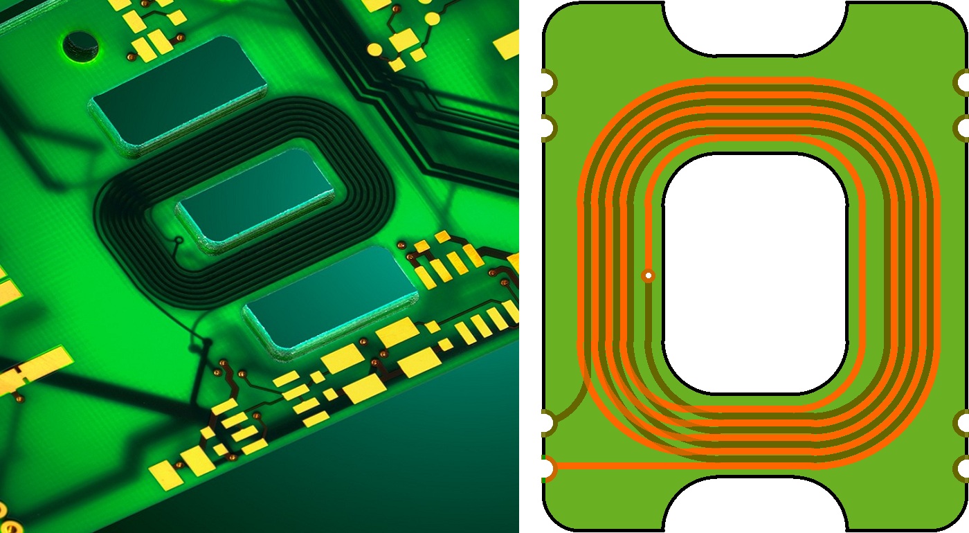
Blog Planar Transformers
Further information about “Coils/Planar transformers” can be found here in this Blog Planar transformers: Understanding and using technology Part I: The basics
Our Technical Support Team and project engineers will be happy to discuss the material, layer buildup, and layout with you from the perspective of impedance and coils/planar transformers.
Keywords
- Multilayer
- Planar transformers
- Foil construction
- Layer count
- Prepregs
- Design to Cost
- Layer stackups