
3.11 Double-Sided PCB | Design Rules
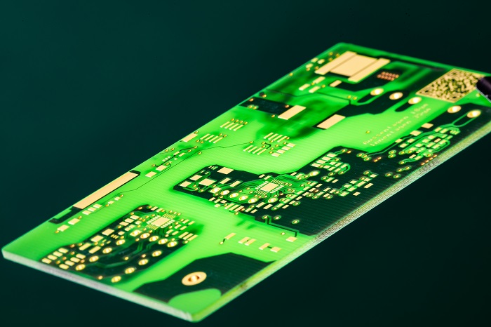
For many applications, it is still sufficient to use low-cost PCB technologies based on a standard FR4 base material. When PCBs are produced in this way, the layout is located on two electrically connected copper layers.
Capabilities
| Feature |
Standard
Design to Cost |
Advanced
|
Learn more |
|---|---|---|---|
| Materials | FR4 UL-Approval overview |
--- | |
| Glass transition temperature of base materials [°C] |
135; 150 | 180 | |
| PCB-final thickness [mm] (incl. final copper and solder mask) |
0.90; 1.10; 1.30; 1.65; 2.10; 2.50; 3.30 | 0.60; other final thicknesses upon request |
|
| Tolerance PCB-final thickness | For final thickness < 1.00 mm ± 0.10 mm For final thickness ≥ 1.00 mm and ≤ 2.00 mm ± 10 % For final thickness > 2.00 mm ± 0.20 mm |
--- | |
| Final copper outer layer [µm] | 18 - 140 | 140 - 210 | |
| Advanced technology | --- | Filled and capped via | |
| Usable production area/ format [mm] |
578 × 498; 573 × 500 578 × 428; 573 × 426 |
--- |
It is always advisable to keep the construction and design rules as as much as possible and as minimum as necessary.
This guarantees optimum Design to Cost.
This guarantees optimum Design to Cost.
Keywords
- Two-layer PCBs