
6.1 Markings | General
In this article:
In accordance with customer requirements, manufacturer markings (such as UL markings, the manufacturer’s logo, date code, etc.) can be applied to the PCB.
We recommend using an inverse approach in the solder mask or (if available) in the silkscreen printing. If the marking is created using copper, the fields must be clearly specified to avoid violating insulation spacing requirements. In addition, the required field size depends on the thickness of the base copper to be etched.
The following marking options are available:
- Marking applied over copper surfaces or over base material using solder mask. A minimum width of 70 µm must be observed as far as the solder mask dams are concerned.
- Marking applied using the screen printing process: Offset and line widths must be taken into account.
- Marking applied using the ink-jet process: Offers the highest possible resolution.
- Marking applied as copper lettering on the base material or inversely to copper surfaces. In this case, the correct line/space requirements must be observed according to the copper thickness.
We recommend using an inverse approach in the solder mask or (if available) in the silkscreen printing. If the marking is created using copper, the fields must be clearly specified to avoid violating insulation spacing requirements. In addition, the required field size depends on the thickness of the base copper to be etched.
Field specifications for printed markings, mask opening (over base material) & base copper thicknesses ≤ 35 µm
- UL complete: field size 10.4 x 3.5 mm
- KSG logo: field size 3.7 x 1.4 mm
- Date code: field size 4.9 x 1.4 mm
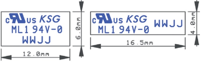
- Entire field: field size 12 x 6 mm or 16.5 x 4 mm depending on arrangement
Examples
Back to top
Keywords
- Marking options
- Markings