
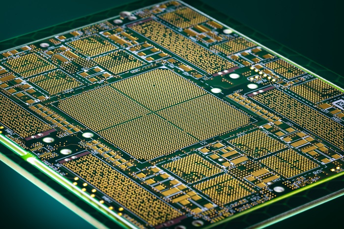
3.1.1 HDI/SBU PCB
Definition of HDI (High-Density-Interconnect-PCB)
- Microvia-Ø ≤ 150 µm
- Hole density > 1,000 vias/dm²
- Line/Space ≤ 125 µm
- Sequential build-up (SBU) using pressing processes
- Blind/buried/stacked/staggered vias
- Al/Au bond surfaces
- Embedded passive/active functionalities
Download_Production-principle_SUB-PCB
Download Production principle of the manufacturing processes of a 1-x-1 SBU (Sequential Build Up)-PCB
Microvia
Microvia holes in combination with through-holesMicrovia
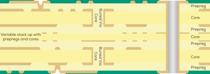
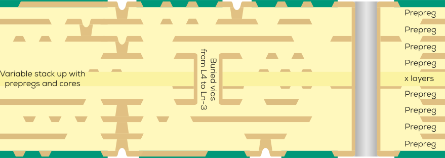
Microvia holes in combination with buried via cores and through-holesSBU 1-x-1
Microvia holes in combination with buried vias and through-holes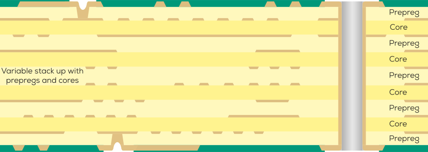
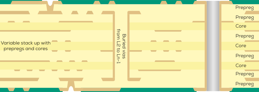

SBU 1-x-1
Two microvia layers in combination with buried vias and through-holesSBU 2-x-2
Microvia over 2 and 3 layers in combination with buried vias and through-holesSBU 2-x-2
Staggered microvia in combination with buried vias and through-holes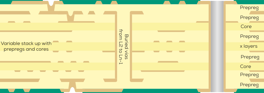
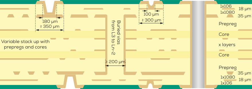


SBU 2-x-2
Stacked microvias in combination with buried vias and through holesSBU 3-x-3
Staggered microvias in combination with buried vias and through holesSBU 3-x-3
Staggered and/or stacked microvias in combination with buried vias and through holes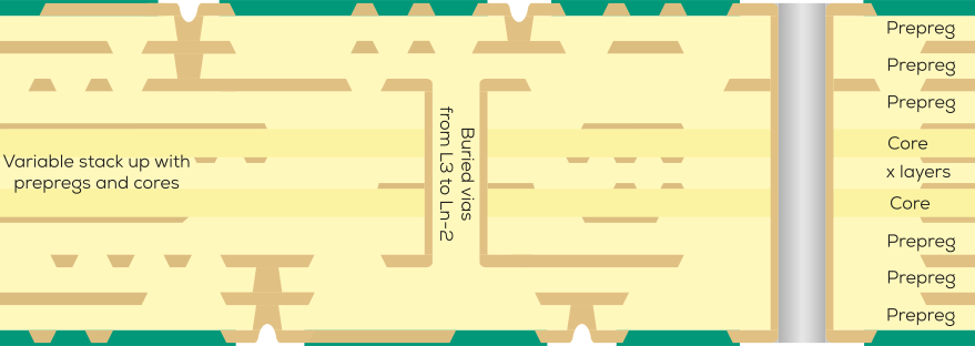
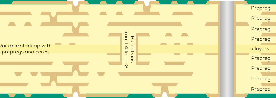

Design to Cost recommendation from KSG:
For SBU (Sequential Build Up) layer structures, it is advisable to design all vias for electrical changeover between the individual layers as Buried Vias in combination with Microvias, if this is possible.
The advantage of this is that if the requirement
"Through vias for reasons such as
- No solder penetration through vias
- Prevention of solder outflow
- Vacuum adaptation
- Sealing for potting varnish
to seal", no additional process such as
11.1 Via Sealing Technology | Single-Sided Plugged Via According To IPC-4761, Type IIIa or
11.3 Via Sealing Technology | Filled and Capped According To IPC-4761, Type VII
is necessary.
Frequently asked questions
What does HDI stand for in the context of printed circuit boards?
The abbreviation HDI stands for “high-density interconnect”. It is used to describe printed circuit boards that have a high packing density and so enable optimum miniaturization to be achieved. Blind vias, microvias, and buried vias are typically used within this context, along with thin conductor widths and narrow conductor spacing. To achieve the HDI properties, the SBU construction method is often used because of its special capabilities. For this reason, both abbreviations – HDI and SBU – frequently appear together.
What does SBU mean in the context of printed circuit boards?
SBU stands for “sequential buildup”. With this method, multilayer PCBs are built up layer by layer (sequentially) in several pressing cycles. In contrast to multilayer PCBs that only undergo pressing once, the SBU approach allows components to be connected to each other in a more complex way, as buried vias (of various designs) can be additionally incorporated as part of the process. As the SBU method generally involves the creation of HDI (high-density interconnection) PCBs, both abbreviations – SBU and HDI – usually appear together.
Keywords
- High-density interconnect (HDI)
- Sequential build-up (SBU)
- Stacked microvias
- Single ply
- Via-in-pad (VIP)
- Prepregs
- Miniaturization
- Vias
- Layer stackups