
2.3 High-Current Solutions
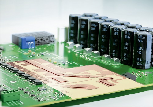
Features & Advantages
- High-current control and power electronics on one board
- Targeted partial cross-section enlargement for high-current paths for currents up to several hundred amperes
- Minimization of the space required for high-current conductors
- High current in combination with 3D installation geometries
- Reduction of total costs (logistics, procurement, assembly, quality assurance)
- Design support and calculation of current paths
Heavy copper PCB
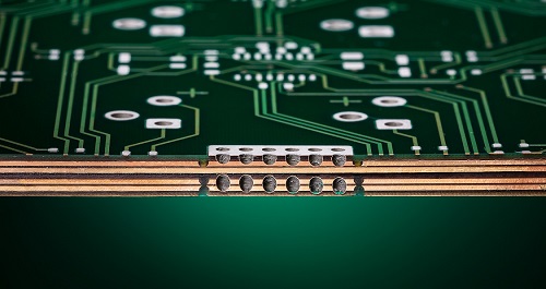
Iceberg PCB
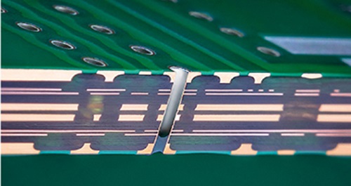
HSMtec® PCB
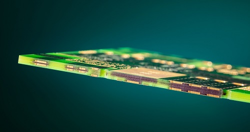
Starting with your initial product idea, our Technical Support Team will be happy to advise you every step of the way as they work with you to find the most suitable PCB solution.
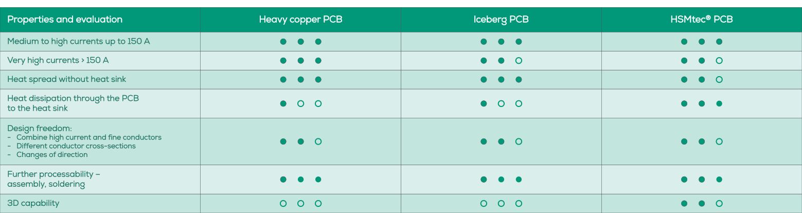
With a heavy copper PCB, copper plating thicknesses of up to 400 µm can be achieved using conventional etching technology. As a result, large copper cross-sectional areas for electricity or heat can be realized efficiently while selectively reducing power dissipation. This type of product can be designed as either a multilayer PCB or a double-sided PCB.
Learn more
Learn more
An Iceberg PCB enables the partial creation of copper traces with a thickness of up to 400 µm on outer layers with 105 µm standard copper. This allows high currents and fine conductors to be combined efficiently in a multilayer with optional inner layers as well.
Learn more
Learn more
The HSMtec® PCB technology enables the partial insertion of large copper cross-sectional areas in any position and layer of a standard FR4 multilayer. Thanks to the vast array of design types, high currents or heat losses from components can be carefully channeled into PCBs – without the need for any further external work steps.
Learn more
Learn more
Comparison of High-Current PCB Technologies
Keywords
- High-current PCBs
- Power electronics
- High current