
1.2 Scope of Data/Data Formats
PCB Data and Documentation
We produce the printed circuit board on the basis of the data you provide as a customer. Therefore, this customer data serves as a specification.
Scope of Data
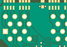
- Information on the PCB topography, e.g., the course of the conductors or the position of the solder and SMD pads
- Drill files (example format: Excellon or Sieb&Meyer)
- Specification of product-relevant features (e.g., material thickness, copper cladding)
- Information on deviations from the customer standard
- Drawing with details of all mechanical processing operations (scoring lines, countersinks, cut-outs, etc.)
Data Formats
| Data formats | Additional information is required for some data formats |
|---|---|
| Gerber RS-274-X | --- |
| Gerber X2 | --- |
| ODB++ | --- |
| DPF | --- |
| IPC-2581 | --- |
| Gerber RS-274-D | Aperture description |
| HPGL/DXF | Specification of the pin widths |
| Eagle | Specification of the Eagle version, layer allocation list, indication of the layers to be output |
Frequently asked questions
Are SMD (solder-mask-defined) pads commonly used? How should these be included in the data if the PCB features both SMD pads and classic non-solder mask defined pads (NSMD, sometimes also known as copper-/metal-defined pads)?
Solder-mask defined (SMD) and non-solder mask defined (NSMD) pads are both common. It is up to the layouter to decide which type should be used, with the choice being determined by the layout data of the solder mask. In the case of NSMD pads, there should be an opening of at least 50 µm in the solder mask around the pad. By contrast, in the case of SMD pads, the solder mask should have an overlap measuring at least 20 µm in width all the way around in the border area of the copper pad so that one part of the copper pad is effectively covered by the solder mask.
Is ODB++ now a common data format or should preference be given to the classic Gerber data format?
Yes, ODB++ is a common data format and can be easily processed as an alternative to Gerber.
In what format should the board outline be provided?
Preferably, it should be supplied as Gerber data with a matching drawing.
Keywords
- Gerber data
- ODB++
- IPC-2581
- Drill data
- Board outline
- DXF
- PCB data