
3.5.1 Iceberg PCB
General
Back to top
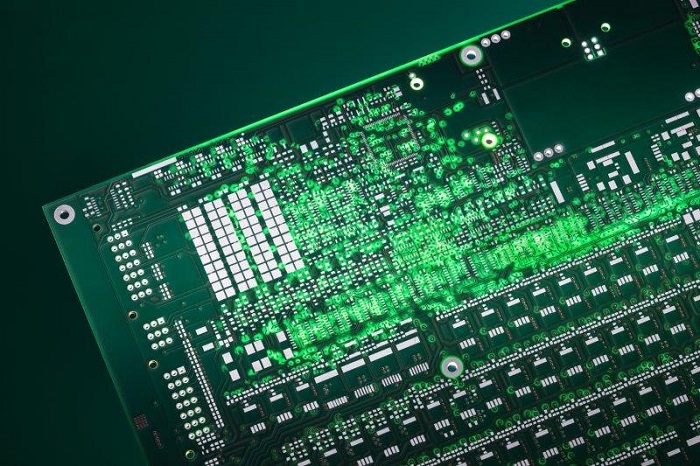
The Iceberg PCB is characterized by stackups with mixed copper thicknesses of 105 µm and 400 µm in outer layers with uniform surface topography. High currents and fine conductors can be efficiently combined in one multilayer with optional inner layers.
Features & Advantages
- High currents and heat spread in the PCB
- High currents and control electronics in one board
- Use of standard materials/technologies
- Can undergo further processing using the standard assembly process
- Lower costs thanks to the elimination of additional connection technology and manual work steps
- Increased system reliability
Download_Production-principle_Iceberg-technology
Download
Current-carrying capacity - you can use our free tool Online High-current calculator to calculate the conductor cross-section or design width required for the respective high-current conductor for several PCB technologies. All you have to do is enter a few details. In addition, our Technical Support Team will be happy to assist you with the processes of dimensioning your high-current conductors and selecting the most suitable PCB technology.
Keywords
- Iceberg technology
- Selective heavy copper
- High current
- Copper thickness