
9.1 Solder Mask
In this article:
The solder mask protects the surface against mechanical or chemical influences (corrosion) and prevents short circuits during soldering. It insulates the PCB surface from other elements (e.g., components or enclosures) while optimizing electrical properties (by increasing the flashover voltage).
Data to Be Supplied
The openings of the individual soldering areas should be as large as the soldering area (“zero opening”). In accordance with the tolerances in our manufacturing processes, we increase the opening of the soldering surfaces by 50 µm (all the way around) as standard.
Standard Photosensitive Solder Mask
Special Colors
| Feature | Value |
|---|---|
| Solder mask lacquer type | SUN Chemical Circuit
|
| Solder mask lacquer type | Peters Elpemer SD 2491 SG-TSW, white |
| Solder mask lacquer type | Taiyo PSR 9000 flexible solder mask, green |
| Solder mask color | Blue, white, black, red, yellow, flexible solder mask only available in green |
| Dielectric strength | Material-specific (see material data sheets) |
| Comparitive tracking index CTI | Material-specific (see material data sheets) |
(*) Attention, solder resist type being discontinued!
| Code | Description | Standard Design to Cost | Advanced |
|---|---|---|---|
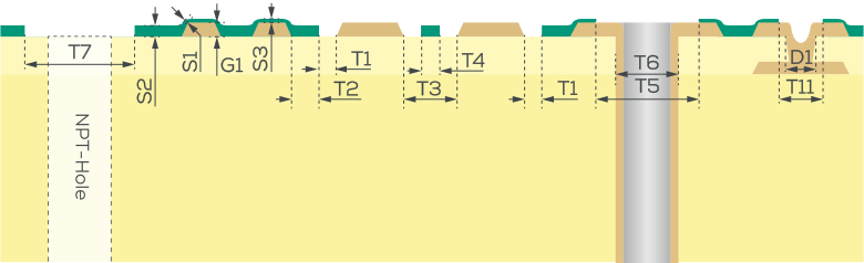
| G1 | Cu thickness of final copper outer layer [µm] | < 50 | ≥ 50 |
| S1 | Thickness of solder mask on edge of copper [µm] | > 5 | ≥ 5 |
| S2 | Thickness of solder mask on base material [µm] | 35 - 60 | ≤ 140 |
| S3 | Thickness of solder mask on conductor [µm] | 6 - 40 | ≤ 120 |
Frequently asked questions
Are SMD (solder-mask-defined) pads commonly used? How should these be included in the data if the PCB features both SMD pads and classic non-solder mask defined pads (NSMD, sometimes also known as copper-/metal-defined pads)?
Solder-mask defined (SMD) and non-solder mask defined (NSMD) pads are both common. It is up to the layouter to decide which type should be used, with the choice being determined by the layout data of the solder mask. In the case of NSMD pads, there should be an opening of at least 50 µm in the solder mask around the pad. By contrast, in the case of SMD pads, the solder mask should have an overlap measuring at least 20 µm in width all the way around in the border area of the copper pad so that one part of the copper pad is effectively covered by the solder mask.
Keywords
- Solder mask
- Solder mask colors
- Solder mask defined (SMD)
- Solder mask dams
- Via tenting
- PCB data
- Via sealing
- Design guidelines